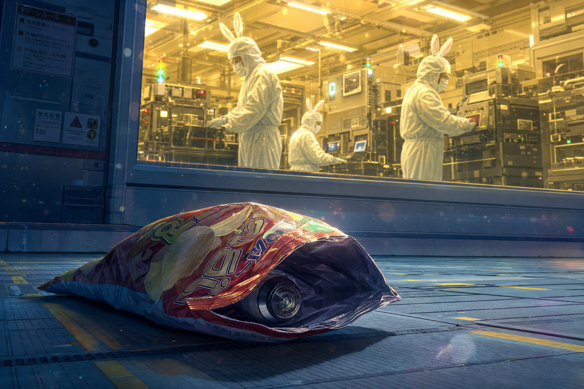
南亞科技的前工程師把相機藏在零食袋裡,準備帶著竊取的DRAM機密出境。這個細節讓人想起那種老派間諜電影的道具——但起訴的時間點,恰好夾在兩則完全不同尺度的新聞之間:台塑集團與日本大賽璐(Daicel)宣布組建50-50合資公司,聯合生產電子級光刻劑稀釋液;矽品精密在雲林破土,興建CoWoS先進封裝廠。
一個人的貪念,放在這個框架裡,顯得格外渺小——也格外說明了問題。
被低估的那一層
台灣半導體的討論,長年集中在晶圓代工製程、先進封裝、HBM記憶體這些主舞台。材料這一層,幾乎是系統性地被忽略。但SEMI Taiwan的數據說得很清楚:台灣連續16年為全球最大半導體材料消費國,2025年採購金額達217億美元,占全球732億美元採購總量的30%。
這個比例從未讓業外人士驚呼——因為材料不拍照,不發布會,不像晶片那樣有具體型號可以報導。
偏偏材料是卡脖子最安靜的地方。ASE日月光明確表示,現有材料產能只能滿足客戶需求不到50%。這不是產線不夠快,是材料根本跟不上。AI算力的瓶頸,從製程端往上游移動,正在向材料端收攏。
台塑×Daicel:石化資產的半導體轉化
電子級光刻劑稀釋液是高純度電子化學品,過去這個品類的供應鏈由日本與德國業者主導。台塑集團的優勢在石化垂直整合,Daicel則是全球光刻劑材料的主要供應商之一。50-50的持股結構讓這筆合資變成技術移轉與在地生產能力的共同綁定。
對照TSMC-Sony在日本熊本的晶圓廠合作,台日半導體同盟的合作面向,正從晶圓代工延伸進入前端化工材料。這個補完是刻意的:若台灣能在材料端降低對歐洲供應商(如BASF、默克)的依賴,同時把日本技術留在台日合作框架內,整條供應鏈的抗干擾能力就往上走了一個等級。
合資廠的選址與量產時程目前尚未完整披露,但方向已定。
矽品在雲林,以及去中化邏輯的完整面
矽品精密(SPIL)在雲林興建CoWoS先進封裝廠,是AMD百億美元AI生態系布局的核心節點之一。CoWoS是台積電的先進封裝技術,將高頻寬記憶體與處理器整合在同一個封裝基板上——算力密度的躍升,很大程度來自這道工序,不是來自製程微縮。
封裝廠落地雲林,代表AI供應鏈的物理足跡正在向台灣中部延伸。這在產業地理上是個值得追蹤的移動,因為一旦封裝產能在地化,對封裝用特殊基板、特殊氣體、化學品的在地採購需求也會跟著升級。台塑×Daicel的材料布局,與矽品的封裝擴張,在這條邏輯鏈上並不是兩件分開的事。
零食袋說明了什麼
把相機藏進洋芋片袋,不是什麼高明的手法,但說明了一件事:技術機密的滲出風險,始終存在於供應鏈最末端——那個已知道製程細節的個別工程師。南亞科技DRAM技術被竊取的案例,在台灣半導體技術外流的起訴紀錄裡並非孤例。
宏觀格局愈強固,個人層次的漏洞就愈顯眼。台日材料合資可以透過法律架構管控技術流向,台灣研擬收緊AI晶片對外出口限制可以設定邊界,但洋芋片袋裡的相機,沒有任何供應鏈設計能事先預防。
這三件事同時存在,是台灣半導體生態真實的剖面——宏觀布局精密,個人風險裸露,材料層長期被低估。SEMI Taiwan材料聯盟在2026年8月啟動,把這個一直存在但很少被正視的缺口,第一次變成了白紙黑字的集體目標。
217億美元的材料採購,30%的全球份額,不到50%的供需滿足率。這些數字過去安靜地藏在產業報告裡,現在被一紙聯盟章程拉進了公開討論。
— 溫以君
A Camera in a Chip Bag and a 50-50 Joint Venture
A former engineer at Nanya Technology was indicted for smuggling trade secrets — DRAM process data — concealed inside a snack bag with a hidden camera. The image is almost cartoonish. But the timing places it squarely between two announcements operating at a completely different scale: Formosa Plastics Corp. and Japan’s Daicel Corp. signing a 50-50 joint venture to produce electronic-grade photoresist thinner, and SPIL breaking ground on a CoWoS advanced packaging plant in Yunlin County.
One person’s greed, set against those two events, says something precise about where the vulnerabilities actually live.
The Layer Nobody Talks About
Taiwan’s semiconductor conversation gravitates toward leading-edge processes, advanced packaging, and HBM. Materials — the chemicals, gases, and specialty compounds that make any of that possible — sit in the background, chronically underreported. The numbers are stark: Taiwan has been the world’s largest semiconductor materials consumer for 16 consecutive years. In 2025, procurement reached US$21.7 billion, or roughly 30% of the global total of US$73.2 billion.
That share has never generated much outside attention, because materials don’t have model numbers or keynote presentations. They don’t photograph well.
ASE’s admission that existing materials capacity can satisfy less than 50% of customer demand reframes the AI bottleneck conversation. The constraint has moved from fab throughput upstream into the chemicals and substrates that enable advanced packaging in the first place. The SEMI Taiwan Materials Alliance, launched in August 2026, made this gap explicit for the first time in an organized, industry-wide format.
What Formosa Plastics and Daicel Are Actually Building
Electronic-grade photoresist thinner is a high-purity specialty chemical. Until now, that segment was dominated by Japanese and German suppliers. Formosa Plastics brings deep petrochemical vertical integration; Daicel is one of the world’s primary photoresist materials suppliers. The 50-50 equity split makes this a mutual lock-in of technology transfer and local production capability.
Against the backdrop of the TSMC-Sony wafer fab partnership in Kumamoto, the Taiwan-Japan semiconductor alliance is expanding its scope from wafer fabrication into front-end chemical materials. This joint venture reaches volume production, it would begin reducing Taiwan’s dependence on European specialty chemical suppliers while keeping Japanese process chemistry inside a bilateral framework. The site and production timeline have not been fully disclosed, but the structural logic is already visible.
SPIL’s CoWoS plant in Yunlin is a separate but connected move. CoWoS packaging integrates high-bandwidth memory and processors on the same substrate — that’s where a significant portion of AI compute density gains are coming from, not from further process shrinks alone. A packaging plant in Yunlin creates downstream pull for specialty substrates, gases, and chemicals sourced locally. The Formosa-Daicel materials play and the SPIL packaging expansion are not independent stories on this supply chain map.
The Snack Bag Problem
Hiding a camera inside a chip bag is not a sophisticated exfiltration method. It is, however, a reliable reminder that the final vulnerability in any supply chain is the individual who already knows the process details. Cases of semiconductor IP theft in Taiwan’s indictment record are not rare — this one draws attention because the method was so mundane.
Joint ventures can be structured to control technology flow across borders. Export restrictions can define boundaries at the system level. Neither instrument reaches the engineer walking out with a camera and a bag of snacks.
All three events — the material joint venture, the packaging plant groundbreaking, the trade secret indictment — describe the same ecosystem at three different resolutions. The macro architecture is becoming more deliberate. The individual exposure layer remains ungoverned by design. And the materials tier, which quietly accounts for nearly a third of global semiconductor materials spending, is only now being treated as a strategic object rather than a procurement line item.
US$21.7 billion. Less than 50% supply coverage. Sixteen years as the world’s largest buyer, with almost no public conversation about what that dependency actually means.
— 溫以君
延伸閱讀
https://justfly.idv.tw/s/TX2T748